Optical Profilometry
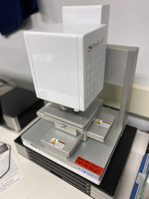
| Profilm 3D Optical Profilometer [SOP] |
|---|
| Objectives: 10x, 20x, 50x |
| Field of View: 2.0 x 1.7 mm (10x), 1.0 x 0.85 mm (20x), 0.4 x 0.34 mm (50x) |
| Surface Roughness Resolution: 0.05μm |
| Stage XY range: 100 mm x 100 mm |
| Z range: 100 mm |
| Camera: 2592 x 1944 (5 megapixels) |
The Profilm 3D optical profilometer uses white light interferometry to measure surface profiles and roughness. It has 10x, 20x, and 50x objectives that can resolve surface roughness down to 0.05 μm.
Introduction
Profilometry is a technique used to extract topographical data from a surface. [1] This can be a single point, a line scan or even a full three dimensional scan. The purpose of profilometry is to get surface morphology, step heights and surface roughness. This can be done using a physical probe or by using light. Metrology is the science of measurement. How rough is the sample? How high are the features? How much of the area has voids or particles? What is the defect density? Answers to these questions are often quantified using profilometry. All profilometers consist of at least two parts – a detector and a sample stage. The detector is what determines where the points on the sample are and the sample stage is what holds the sample. In some systems, the sample stage moves to allow for measurement while in others the detector moves. There are also instruments where both the sample stage and detector move.
Principle
Stylus Profilometry
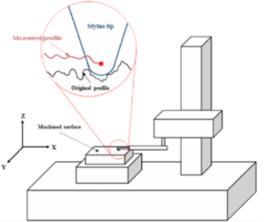
Stylus profilometers use a probe to detect the surface, physically moving a probe along the surface in order to acquire the surface height. This is done mechanically with a feedback loop that monitors the force from the sample pushing up against the probe as it scans along the surface. A feedback system is used to keep the arm with a specific amount of torque on it, known as the ‘setpoint’. The changes in the Z position of the arm holder can then be used to reconstruct the surface. Stylus profilometry requires force feedback and physically touching the surface, so while it is extremely sensitive and provides high Z resolution, it is sensitive to soft surfaces and the probe can become contaminated by the surface. This technique can also be destructive to some surfaces. Because a stylus profilometer involves physical movements in X, Y and Z while maintaining contact with the surface, it is slower than non-contact techniques. The stylus tip size and shape can influence the measurements and limit the lateral resolution.
Optical Profilometry
Optical profilometry uses light instead of a physical probe. This can be done a number of ways. The key component to this technique is directing the light in a way that it can detect the surface in 3D. Examples include optical interference, using a confocal aperture, focus and phase detection, and projecting a pattern onto the optical image.
White Light Interferometry
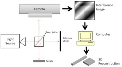
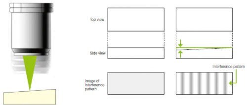
Light interference occurs when there is a difference in distance traveled by the light (light path) from the surface of a target object to a certain point; a white light interferometer uses this phenomenon to measure the surface roughness of a sample [2]. The light emitted from the source (semiconductor laser, etc.) is separated into reference and measurement beams. While the reference beam is passed through the reference mirror through a half mirror, the measurement beam is reflected and guided to the sample surface. The passed beam is reflected by the reference mirror to the charge-coupled device (CCD) image sensor and forms an interference pattern. The other beam is reflected off the sample surface, passes the half mirror, and forms an image through the CCD image sensor. The white light interferometer is designed so that the optical path length from the CCD element to the reference mirror and that from the CCD element to the sample surface are the same. The asperity on the sample surface causes these path lengths to be unequal, which results in forming an interference pattern at the CCD element. The number of lines in the interference pattern is translated to peaks and troughs (heights) on the sample surface.
Advantages
- Capable of measuring a wide field of view: Measurement in sub-nanometer range is possible.
- Quick measurement: Approximately 20 seconds compared to much longer for a stylus profilometer.
Disadvantages
- No or limited angular characteristic
- Use is limited on certain objects: White light interferometers can only measure when there is a good reflection. There, it does not support measurement capabilities on a wide variety of objects. Measurements may also not be possible when there is a significant difference between the light reflected from the reference mirror and light reflected from the measurement area. (White light interferometers handle mirrored surfaces well, but cannot measure spiky or bumpy samples or nonreflective parts.
- Requires tilt correction: Prior to measuring, sample tilt correction must be performed using a goniometric stage. Tilted samples can cause closely-spaced interference patters, which hinder measurement accuracy. Some white light interferometry systems are equipped with a tilt mechanism that automatically corrects the sample tilt.
- Low resolution for XY stage measurements: The resolution for XY stage measurements are low due to the low number of sampling data sets (approximately 300,000). Some white light interferometry systems can scale up to use approximately 980,000 data sets.
- Sensitive to vibrations: Place of installation is limited due to the equipment’s high sensitivity to vibrations. Shock-absorbing tables are necessary for installation.
References
- ↑ Optical Profilometry. Nanoscience Instruments. (2018, July 26). https://www.nanoscience.com/techniques/optical-profilometry/.
- ↑ White Light Interferometers. White Light Interferometers | Instruments Used For Roughness Measurements | Introduction To Roughness | KEYENCE America. (n.d.). https://www.keyence.com/ss/products/microscope/roughness/equipment/interferometers.jsp.


