Scanning Electron Microscopy: Difference between revisions
No edit summary |
No edit summary |
||
| Line 80: | Line 80: | ||
===Astigmatism=== | ===Astigmatism=== | ||
Astigmatism in SEM occurs due to fluctuations in magnetic field strength, which may be caused by defects in the electron column core, source contamination, or magnetic samples. This typically results in the blurring or stretching of the SEM image, and can be corrected using stigmation coils. Most SEMs have both an X and Y stigmator knobs for correcting stretching, as well as an auto-stigmation feature. | Astigmatism in SEM occurs due to fluctuations in magnetic field strength, which may be caused by defects in the electron column core, source contamination, or magnetic samples. This typically results in the blurring or stretching of the SEM image, and can be corrected using stigmation coils. Most SEMs have both an X and Y stigmator knobs for correcting stretching, as well as an auto-stigmation feature. | ||
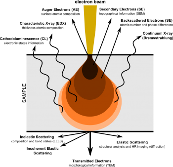
[[File:SEM-EmissionMechanisms.png|350px|thumb|right|SE, BSE, and characteristic X-ray Emissions<br>© Rob Hurt / Wikimedia Commons / CC-BY-SA-4.0]] | [[File:SEM-EmissionMechanisms.png|350px|thumb|right|SE, BSE, and characteristic X-ray Emissions<br>© Rob Hurt / Wikimedia Commons / CC-BY-SA-4.0]] | ||
| Line 100: | Line 99: | ||
=== EBSD === | === EBSD === | ||
==Depth of Field== | ==Depth of Field== | ||
==Common SEM Issues== | ==Common SEM Issues== | ||
Revision as of 14:57, 13 July 2021
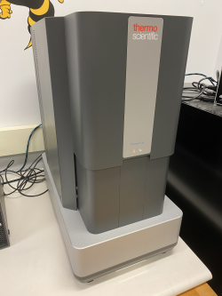
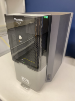
| PhenomXL G2 SEM | Phenom ProX G5 SEM | ||
|---|---|---|---|
| Magnification Range: | 160x to 200,000x | 40,000x to 100,000x | |
| Accelerating Voltages: | 4.8kV to 20kV (advanced mode) | 5, 10, or 15kV | |
| Feature Resolution: | < 50nm | < 500nm | |
| Detectors: | Secondary (SED) & Backscatter (BSD) | Backscatter only | |
| Capabilities: | EDS, AIM, 3DRR | EDS | |
| Sample Dimensions: | < 10cm in diameter, <4cm tall | < 2.5cm in diameter, <3cm tall |
Scanning electron microscopy (SEM) rasters an electron beam across a specific area on a sample, allowing for much higher magnifications compared to optical microscopy. The electrons are either elastically or inelastically reflected off the sample, then captured by detector(s) to yield an image.
Electron Microscopy
Electron and optical microscopy share many fundamental components—specifically, a lens used to focus a specific type of source, and after either reflecting from or transmitting through the sample, a “signal” is then captured by a detector which processes inputs and spits out an image. In optical microscopy, an optical glass lens focuses photons from a lamp into either a digital camera or your eye. In electron microscopy, a series of variable magnetic fields serve as condenser lenses to vary the current and spot size of the electron beam (e-beam) generated from an electron gun. In SEM, this beam is then focused using an electromagnetic objective lens and rastered across the sample by a set of scan coils.
Similar to optical microscopy, electron microscopy also has both reflection and transmission modes—these are two separate imaging techniques known as Scanning Electron Microscopy (SEM) and Transmission Electron Microscopy (TEM), respectively.
Types of Electron Guns
There are 2 main types of electron guns used in electron microscopy: thermionic (Schottky) emission and cold field emission. Both types required an electron source—typically this is either a single crystal of tungsten, lanthanum hexaboride (LaB6), or cerium hexaboride (CeB6). Both Phenom SEMs at the MILL use thermionic emission guns with a CeB6 source.
Magnification & Resolution
SEMs can provide an additional 2 orders of magnitude in magnification and resolution when compared to optical microscopes, which typically max out around 1,000x magnification and 200 nm resolution. SEMs typically have around 100,000x magnification and 2 nm resolution. This additional resolution is governed by the Abbe equation and de Broglie wave equation.
Proof
Abbe’s equation defines the theoretical maximum resolution of a microscope, [math]\displaystyle{ \delta }[/math] as:
- [math]\displaystyle{ \delta=\frac{k\lambda}{n\sin(\alpha)} }[/math],
where [math]\displaystyle{ k = 0.61 }[/math] is an empirical constant, [math]\displaystyle{ n }[/math] is the refractive index, and [math]\displaystyle{ \alpha }[/math] is the aperture half-angle. The term in the denominator, [math]\displaystyle{ n\sin{\alpha)} }[/math], is also known as the numerical aperture, or nA.
In optical microscopy, Abbe’s equation simplifies to [math]\displaystyle{ \delta=\frac{0.61\lambda}{nA} }[/math], where the numerical aperture at high magnifications typically levels out at [math]\displaystyle{ nA \approx 1.35 }[/math]. Plugging in the [math]\displaystyle{ \lambda }[/math] for green light gives:
- [math]\displaystyle{ \delta=\frac{0.61\cdot500\textrm{nm}}{1.35}=226\textnormal{nm} }[/math]
In electron microscopy, the refractive index is typically 1, since the chamber is pumped down to near-vacuum conditions, and the aperture half-angle is typically very small. Using the small angle approximation, we can simplify Abbe’s equation to
- [math]\displaystyle{ \delta=\frac{0.61\lambda}{\alpha} }[/math].
Since electron microscopy uses an electron beam to image the sample, [math]\displaystyle{ \lambda }[/math] is now the de Broglie wavelength of an electron. The de Broglie wave equation states:
- [math]\displaystyle{ \lambda=\frac{h}{p} }[/math],
where [math]\displaystyle{ h }[/math] is Planck’s constant and [math]\displaystyle{ p }[/math] is momentum. Recall that kinetic energy is defined as:
- [math]\displaystyle{ \textrm{KE} = \frac{1}{2}mv^2 }[/math]
- [math]\displaystyle{ \therefore p=mv=\sqrt{2m(\textrm{KE})} }[/math]
Electron microscopes such as SEMs typically have a controllable accelerating voltage—this term affects the kinetic energy of the e-beam by the fundamental relation: [math]\displaystyle{ \textrm{KE} = e\textrm{V} }[/math], where [math]\displaystyle{ e }[/math] is the elementary charge. Plugging in for momentum and kinetic energy, we get:
- [math]\displaystyle{ \therefore \lambda=\frac{h}{\sqrt{2me\textrm{V}}} }[/math]
Finally, by plugging in all constants and assuming a small aperture half-angle of 0.01 rad (must use radians for small angle approximation), the following resolutions can be obtained for varying accelerating voltages. Note that these calculations use Newtonian equations, not Einsteinian (relativistic) equations.
| Accelerating Voltage (kV) | de Broglie Wavelength (nm) | Abbe Resolution (nm) |
|---|---|---|
| 5 | .0173 | 1.06 |
| 10 | .0123 | .751 |
| 15 | .0100 | .613 |
| 100 | .00388 pm | .237 |
Limitations
Despite the near-atomic resolution claimed by Abbe’s equation at higher accelerating voltages, SEMs struggle to reach beyond nanometer-level resolution, and therefore cannot see individual atoms. There are many variables which cause the reduction in practical resolution, so only major factors are listed here.
Interaction Volume
The first limitation is electron interaction volume. When a high energy electron beam strikes the sample, electrons penetrate the sample and knock free other electrons, ballooning into a relatively large interaction volume. The greater the accelerating voltage, the greater the interaction volume—therefore, SEMs must balance the improvement in theoretical Abbe resolution from a higher energy and the decrease in resolution from larger interaction volumes at high accelerating voltages.
Interaction volume typically has a diameter in the micron range for bulk samples and a diameter in the same order as sample thickness for thin foils used in TEM. This tiny interaction volume is also why extremely thin (<50nm) TEM foils can get down to atomic resolution. For SEM samples, noise and overlapping signals from different areas of a sample will blur an image if the accelerating voltage and interaction volume are too large. Ideally, interaction volume diameter should approximate the size of sample features to get sharp images.
Aberrations
Aberrations occur when a lens fails to converge all rays at a single point and the image becomes out of focus. There are two types of aberrations: spherical and chromatic. In SEM, spherical aberrations occur when electrons near the edges of an electromagnetic lens are bent inconsistently compared to electrons at the center of the lens and fail to converge—this can be fixed by using a smaller aperture. Chromatic aberrations occur when the electron beam is not of uniform energy, causing the electromagnetic lens to bend electrons of differing energies to different points on the focal plane. Both of these phenomena derive their names from the same photon-based effects in optical microscopy.
Astigmatism
Astigmatism in SEM occurs due to fluctuations in magnetic field strength, which may be caused by defects in the electron column core, source contamination, or magnetic samples. This typically results in the blurring or stretching of the SEM image, and can be corrected using stigmation coils. Most SEMs have both an X and Y stigmator knobs for correcting stretching, as well as an auto-stigmation feature.
Information Provided by SEM Emissions
When primary electrons (PE) from the e-beam inelastically interact with electrons in the sample, they transfer a significant portion of their kinetic energy to another electron, which is then ejected as a secondary electron (SE). Other times, primary electrons can "slingshot" around atomic nuclei and return while only losing a negligible amount of energy. This is an elastic interaction, and the returned primary electrons are redubbed backscattered electrons (BSD). While SE have energies in the 10s of eVs, BSE return with the same initial energy, which varies based on accelerating voltage (10 kV accelerating voltage [math]\displaystyle{ \Rightarrow }[/math] 10 keV of energy). Therefore, SEMs primarily handle 2 detectors used for imaging: these are the secondary electron detector (SED) and the backscattered electron detector (BSD).
SED
Secondary electrons give an image which shows topographical features and a relatively large depth of field.
Since SEs have such low energies, they can only escape when present in the sample's surface (the top several nm). This also means SEs have low interaction volume, and have resolutions on the nm level. The most common type of SED is the Everhart-Thornley (ET) detector, which are placed off-center from the sample to provide better contrast between SEs coming from different areas on the sample surface in exchange for slightly worse signal-to-noise ratio. The reasoning for sacrificing signal is because SE yields (# of emitted SEs per PE) are over 100%—this is because high-energy PEs undergoing inelastic interactions can dislodge multiple SEs at a time.
BSD
Backscattered electrons give elemental contrast (Z-contrast), but by using a 4-quadrant detector, some topographical features are also resolvable. Turning off half of a 4-quadrant BSD works similarly to ET SEDs, where one side of sample will appear brighter than the other side. Note that these topographical modes do lose some Z-contrast in the process.
BSEs are very high energy, and therefore penetrate deeper into the sample than SEs. This larger interaction volume results in BSD resolutions in the 100s of nm, 2 orders of magnitude worse than SEDs. Additionally, BSE yields are typically under 50% because they cannot "share" their initial energy and some BSEs become trapped in atomic orbitals. Z-contrast occurs because of increasing nucleus size through the periodic table—heavier nuclei will more effectively "slingshot" PEs, result in greater counts for heavier atoms and lower counts for lighter atoms. This is typically displayed by making atomically heavier areas of the sample bright and atomically lighter areas of the sample dark.
EDS
Additionally, inelastic interactions which dislodge secondary electrons leave an electron vacancy which must be quenched, similar to X-ray fluorescence (XRF). The resulting vacancy is quenched, and the surplus energy is ejected as a secondary characteristic X-ray. Since energy drops between electrons levels in a given atom are discrete and distinct, a detector which can catch these secondary X-rays would be able to determine elemental composition. This is known as energy-dispersive X-ray spectroscopy (EDS/EDX), as is very common in SEM systems. Unlike XRF, secondary X-rays are only emitted from a small spot—more specifically, it emits from the interaction volume for characteristic X-rays, which is typically 1-2 μm in diameter with a spot size of a few nm. For comparison XRF depth ranges from several μm to a few mm, and irradiates the entire sample at once.


