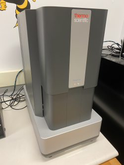
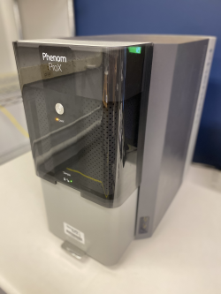
Scanning Electron Microscopy
| PhenomXL G2 SEM | Phenom ProX G5 SEM | ||
|---|---|---|---|
| Magnification Range: | 160x to 200,000x | 40,000x to 100,000x | |
| Accelerating Voltages: | 4.8kV to 20kV (advanced mode) | 5, 10, or 15kV | |
| Feature Resolution: | < 50nm | < 500nm | |
| Detectors: | Secondary (SED) & Backscatter (BSD) | Backscatter only | |
| Capabilities: | EDS, AIM, 3DRR | EDS | |
| Sample Dimensions: | < 10cm in diameter, <4cm tall | < 2.5cm in diameter, <3cm tall |
Scanning electron microscopy (SEM) rasters an electron beam across a specific area on a sample, allowing for much higher magnifications compared to optical microscopy. The electrons are either elastically or inelastically reflected off the sample, then captured by detector(s) to yield an image.
Electron Microscopy
Electron and optical microscopy share many fundamental components—specifically, a lens used to focus a specific type of source, and after either reflecting from or transmitting through the sample, a “signal” is then captured by a detector which processes inputs and spits out an image. In optical microscopy, an optical glass lens focuses photons from a lamp into either a digital camera or your eye. In electron microscopy, a series of variable magnetic fields serve as condenser lenses to focus an electron beam generated from an electron gun.
Similar to optical microscopy, electron microscopy also has both reflection and transmission modes—these are two separate imaging techniques known as Scanning Electron Microscopy (SEM) and Transmission Electron Microscopy (TEM), respectively.
Types of Electron Guns
There are 2 main types of electron guns used in electron microscopy: thermionic (Schottky) emission and cold field emission. Both types required an electron source—typically this is either a single crystal of tungsten, lanthanum hexaboride (LaB6), or cerium hexaboride (CeB6). Both Phenom SEMs at the MILL use thermionic emission guns with a CeB6 source.
Magnification & Resolution
SEMs can provide an additional 2 orders of magnitude in magnification and resolution when compared to optical microscopes, which typically max out around 1,000x magnification and 200 nm resolution. SEMs typically have around 100,000x magnification and 2 nm resolution. This additional resolution is governed by the Abbe equation and de Broglie wave equation.
Proof
Abbe’s equation defines the theoretical maximum resolution of a microscope, [math]\displaystyle{ \delta }[/math] as:
- [math]\displaystyle{ \delta=\frac{k\lambda}{n\sin(\alpha)} }[/math],
where [math]\displaystyle{ k = 0.61 }[/math] is an empirical constant, [math]\displaystyle{ n }[/math] is the refractive index, and [math]\displaystyle{ \alpha }[/math] is the aperture half-angle. The term in the denominator, [math]\displaystyle{ n\sin{\alpha)} }[/math], is also known as the numerical aperture, or nA.
In optical microscopy, Abbe’s equation simplifies to [math]\displaystyle{ \delta=\frac{0.61\lambda}{nA} }[/math], where the numerical aperture at high magnifications typically levels out at [math]\displaystyle{ nA \approx 1.35 }[/math]. Plugging in the [math]\displaystyle{ \lambda }[/math] for green light gives:
- [math]\displaystyle{ \delta=\frac{0.61\cdot500\textrm{nm}}{1.35}=226\textnormal{nm} }[/math]
In electron microscopy, the refractive index is typically 1, since the chamber is pumped down to near-vacuum conditions, and the aperture half-angle is typically very small. Using the small angle approximation, we can simplify Abbe’s equation to
- [math]\displaystyle{ \delta=\frac{0.61\lambda}{\alpha} }[/math].
Since electron microscopy uses an electron beam to image the sample, [math]\displaystyle{ \lambda }[/math] is now the de Broglie wavelength of an electron. The de Broglie wave equation states:
- [math]\displaystyle{ \lambda=\frac{h}{p} }[/math],
where [math]\displaystyle{ h }[/math] is Planck’s constant and [math]\displaystyle{ p }[/math] is momentum. Recall that kinetic energy is defined as:
- [math]\displaystyle{ \textrm{KE} = \frac{1}{2}mv^2 }[/math]
- [math]\displaystyle{ \therefore p=mv=\sqrt{2m(\textrm{KE})} }[/math]
Electron microscopes such as SEMs typically have a controllable accelerating voltage—this term affects the kinetic energy of the electron beam by the fundamental relation: [math]\displaystyle{ \textrm{KE} = e\textrm{V} }[/math], where [math]\displaystyle{ e }[/math] is the elementary charge. Plugging in for momentum and kinetic energy, we get:
- [math]\displaystyle{ \therefore \lambda=\frac{h}{\sqrt{2me\textrm{V}}} }[/math]
Finally, by plugging in all constants and assuming a small aperture half-angle of 0.01 rad (must use radians for small angle approximation), the following resolutions can be obtained for varying accelerating voltages. Note that these calculations use Newtonian equations, not Einsteinian (relativistic) equations.
| Accelerating Voltage (kV) | de Broglie Wavelength (nm) | Resolution (nm) |
|---|---|---|
| 5 | .0173 | 1.06 |
| 10 | .0123 | .751 |
| 15 | .0100 | .613 |
| 100 | .00388 pm | .237 |

